Quantcast
Channel: C2000™︎ 微控制器论坛 - 最近的话题
Viewing all 12114 articles
Browse latest View live

使用CCS5.5和ccs3.3连接f28035开发板的自带仿真器xds100都不成功,是不是开发板坏了?

$
0
0

[Start]

Execute the command:

%ccs_base%/common/uscif/dbgjtag -f %boarddatafile% -rv -o -F inform,logfile=yes -S pathlength -S integrity

[Result]


-----[Print the board config pathname(s)]------------------------------------

C:\Users\yfc\AppData\Local\.TI\2775666225\
0\0\BrdDat\testBoard.dat

-----[Print the reset-command software log-file]-----------------------------

This utility has selected a 100- or 510-class product.
This utility will load the adapter 'jioserdesusb.dll'.
The library build date was 'Apr 1 2013'.
The library build time was '23:55:08'.
The library package version is '5.1.73.0'.
The library component version is '35.34.40.0'.
The controller does not use a programmable FPGA.
The controller has a version number of '4' (0x00000004).
The controller has an insertion length of '0' (0x00000000).
This utility will attempt to reset the controller.
This utility has successfully reset the controller.

-----[Print the reset-command hardware log-file]-----------------------------

The scan-path will be reset by toggling the JTAG TRST signal.
The controller is the FTDI FT2232 with USB interface.
The link from controller to target is direct (without cable).
The software is configured for FTDI FT2232 features.
The controller cannot monitor the value on the EMU[0] pin.
The controller cannot monitor the value on the EMU[1] pin.
The controller cannot control the timing on output pins.
The controller cannot control the timing on input pins.
The scan-path link-delay has been set to exactly '0' (0x0000).

-----[The log-file for the JTAG TCLK output generated from the PLL]----------

There is no hardware for programming the JTAG TCLK frequency.

-----[Measure the source and frequency of the final JTAG TCLKR input]--------

There is no hardware for measuring the JTAG TCLK frequency.

-----[Perform the standard path-length test on the JTAG IR and DR]-----------

This path-length test uses blocks of 512 32-bit words.

The test for the JTAG IR instruction path-length failed.
The JTAG IR instruction scan-path is stuck-at-ones.

The test for the JTAG DR bypass path-length failed.
The JTAG DR bypass scan-path is stuck-at-ones.

-----[Perform the Integrity scan-test on the JTAG IR]------------------------

This test will use blocks of 512 32-bit words.
This test will be applied just once.

Do a test using 0xFFFFFFFF.
Scan tests: 1, skipped: 0, failed: 0
Do a test using 0x00000000.
Test 2 Word 0: scanned out 0x00000000 and scanned in 0xFFFFFFFF.
Test 2 Word 1: scanned out 0x00000000 and scanned in 0xFFFFFFFF.
Test 2 Word 2: scanned out 0x00000000 and scanned in 0xFFFFFFFF.
Test 2 Word 3: scanned out 0x00000000 and scanned in 0xFFFFFFFF.
Test 2 Word 4: scanned out 0x00000000 and scanned in 0xFFFFFFFF.
Test 2 Word 5: scanned out 0x00000000 and scanned in 0xFFFFFFFF.
Test 2 Word 6: scanned out 0x00000000 and scanned in 0xFFFFFFFF.
Test 2 Word 7: scanned out 0x00000000 and scanned in 0xFFFFFFFF.
The details of the first 8 errors have been provided.
The utility will now report only the count of failed tests.
Scan tests: 2, skipped: 0, failed: 1
Do a test using 0xFE03E0E2.
Scan tests: 3, skipped: 0, failed: 2
Do a test using 0x01FC1F1D.
Scan tests: 4, skipped: 0, failed: 3
Do a test using 0x5533CCAA.
Scan tests: 5, skipped: 0, failed: 4
Do a test using 0xAACC3355.
Scan tests: 6, skipped: 0, failed: 5
Some of the values were corrupted - 83.3 percent.

The JTAG IR Integrity scan-test has failed.

-----[Perform the Integrity scan-test on the JTAG DR]------------------------

This test will use blocks of 512 32-bit words.
This test will be applied just once.

Do a test using 0xFFFFFFFF.
Scan tests: 1, skipped: 0, failed: 0
Do a test using 0x00000000.
Test 2 Word 0: scanned out 0x00000000 and scanned in 0xFFFFFFFF.
Test 2 Word 1: scanned out 0x00000000 and scanned in 0xFFFFFFFF.
Test 2 Word 2: scanned out 0x00000000 and scanned in 0xFFFFFFFF.
Test 2 Word 3: scanned out 0x00000000 and scanned in 0xFFFFFFFF.
Test 2 Word 4: scanned out 0x00000000 and scanned in 0xFFFFFFFF.
Test 2 Word 5: scanned out 0x00000000 and scanned in 0xFFFFFFFF.
Test 2 Word 6: scanned out 0x00000000 and scanned in 0xFFFFFFFF.
Test 2 Word 7: scanned out 0x00000000 and scanned in 0xFFFFFFFF.
The details of the first 8 errors have been provided.
The utility will now report only the count of failed tests.
Scan tests: 2, skipped: 0, failed: 1
Do a test using 0xFE03E0E2.
Scan tests: 3, skipped: 0, failed: 2
Do a test using 0x01FC1F1D.
Scan tests: 4, skipped: 0, failed: 3
Do a test using 0x5533CCAA.
Scan tests: 5, skipped: 0, failed: 4
Do a test using 0xAACC3355.
Scan tests: 6, skipped: 0, failed: 5
Some of the values were corrupted - 83.3 percent.

The JTAG DR Integrity scan-test has failed.

怎样在sys/bios下配置芯片定时器

$
0
0

想测试swi响应中断所需时间,在主函数启动定时后进入Bios运行错误,无法记录机械周期数,请问该怎么解决?还有BIOS的频率似乎和CPU的不一样,该怎么设置?

在DSP28377上如何从CLA协处理器触发CPU高级中断??

$
0
0
        我之前在DSP28377S上通过外设中断或软件使能都可以触发CLA协处理器工作了!
        目前主要是考虑到CLA协处理器处理完后与外部芯片如FPGA的数据交互;又该数据交互通过EMIF完成,而CLA又不能直接访问EMIF外设。所以只能考虑通过CPU将数据经EMIF写入到FPGA。
        之前通过CLA协处理器对管脚A的操作输出一个脉冲,管脚A连接管脚B,而管脚B又作为外部中断1的输入管脚,所以,通过该方法可以实现从CLA协处理器触发一个CPU中断。
        但是,通过外部管脚而触发中断的话有将近300ns的延迟,又耗费管脚,可以的话希望能够在CLA中直接设置相应的标志或寄存器来触发CPU中的高级中断,如ADCA1/ADCB1/ADCC1/TIMER0/EINT1/2等从而可以将CLA协处理器中的数据即时地写入到外部FPGA上。
        今天通过设置EPWM.CPMA的值为>EPWM.PRD(在EPWM中断中)和EPWM.CPMA=EPWM.TBCTR(在CLA协处理器中)来触发EPWM中断,中断函数的计数器可以进入的,但是问题是:CLA协处理器的计数器数值会比EPWM中断中的计数器数值要大,按照预期是一样的或最多相差一个计数值而已。
        基于以上问题,恳请高手帮助一起分析指导,谢谢!

XDS100 V3连接TMS320F28027失败

$
0
0

您好,我开发环境 是CCS6,想用XDS100V3仿真28027,但是一直出现如下的错误警告,这个怎么解决呢?

C28xx: Error connecting to the target: (Error -516 @ 0x0) The user selected specific frequency failed the scan-path reliability test. The utility or debugger requested the JTAG controller and cable, that generate the JTAG clock, to provide a user selected fixed frequency.  The built-in scan-path reliability test has failed. This indicates that the JTAG controller and its cable cannot reliably communicate with the target system at that frequency. (Emulation package 5.1.450.0) 

电机空载启动抖动问题(drv8301 revd)

$
0
0

仿照drv8301 revd做了一块电路板。

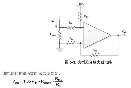
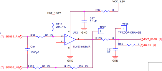
为了测量双向电流( 即正电流和负电流) , 需要使用 1.65V 基准电压,现在1.65V是精准的,但是经过运放TLV2781后,电机不运行时,运放TLV2781输出却偏离了1.65V,有的TLV2781输出为1.67V,有的TLV2781输出为1.62V,此时电机启动可能会有抖动。如果运放TLV2781输出在1.645V到1.655V之间则电机启动不会抖动。电路图及其计算方法如下。

1、经过反复验证,运放TLV2781输出偏离了1.65V是由于运放TLV2781本身不一致导致(理论上在电流为零时输出电压为1.65V),更换运放TLV2781使输出电压在1.65V附近可以解决抖动,大家都说软件偏移可以校准,但是软件校准怎么做啊?请求指点,非常感谢。使用硬件太浪费TLV2781。

2、HAL_cal(HAL_Handle handle),HAL_AdcOffsetSelfCal(handle);这两个函数代表什么意思?请求指点,非常感谢。电机运行前执行HAL_AdcOffsetSelfCal(handle);能不能避免电机抖动问题?具体代码及说明如下:

void HAL_cal(HAL_Handle handle)

 {  

    HAL_Obj *obj = (HAL_Obj *)handle;

// enable the ADC clock   CLK_enableAdcClock(obj->clkHandle);

// Run the Device_cal() function  

 // This function copies the ADC and oscillator calibration values from TI reserved  OTP into the appropriate trim registers  

 // This boot ROM automatically calls this function to calibrate the interal   oscillators and ADC with device specific calibration data.

  // If the boot ROM is bypassed by Code Composer Studio during the development process,   // then the calibration must be initialized by the application

  ENABLE_PROTECTED_REGISTER_WRITE_MODE;

  (*Device_cal)();  

 DISABLE_PROTECTED_REGISTER_WRITE_MODE;

  // run offsets calibration in user's memory  

  HAL_AdcOffsetSelfCal(handle);

  // run oscillator compensation

   HAL_OscTempComp(handle);

  // disable the ADC clock

  CLK_disableAdcClock(obj->clkHandle);

  return;

} // end of HAL_cal() function

CCS中280049M.ccxml的flash烧写配置问题

$
0
0

all:

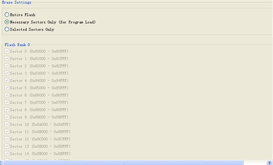
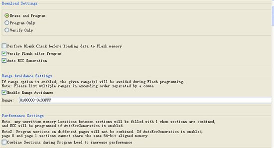
      我想保留flash blank0中0x80000-0x83FFF 的flash做eeprom和在线升级代码,那么我们在ccs中的.ccxml这样配置是否可以, 那个Erase Seting中的这部分0x80000-0x83FFF 地址需要勾掉吗?的具体配置见下图:

【SCI】同样的程序,其他的板子可以,我的板子却不行,忘指点迷津

$
0
0

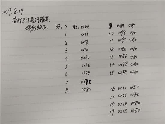
我发送的是int16型变量,电脑端串口助手接收的却变成这样

关于DSP28335控制LCD12864的问题

$
0
0

你好,在一个LCD12864的控制程序中看到一段

#include"DSP2833x_Device.h"
#include "DSP2833x_Examples.h"

#define LCD_DATA_BUS (*((volatile Uint16 *)0x4000))

#define EN GpioDataRegs.GPBDAT.bit.GPIO54
#define RW GpioDataRegs.GPBDAT.bit.GPIO56
#define RS GpioDataRegs.GPBDAT.bit.GPIO57

#define uchar unsigned char

extern uchar menu1[]={"选择电机定时设置"};
extern uchar menu2[]={"时间设置1"};
extern uchar menu3[]={"时间设置2"};
extern uchar menu4[]={"时间设置3"};

void LCDInit(void);
void Write_order(uchar order);
void Write_data(uchar data);
void delay(uchar t);
void configio(void);
void InitXintf(void);
void display(void);

void LCD_DATA (uchar d)
{
  LCD_DATA_BUS = d;

}

其中#define LCD_DATA_BUS (*((volatile Uint16 *)0x4000))应该是定义了八个数据传输口,但是不太了解这句话怎么对应的引脚,求解释一下,多谢了


CCS 编译问题 unresolved symbols remain

$
0
0

error #10234-D: unresolved symbols remain
error #10010: errors encountered during linking; "F2812_ADC_2.out" not built

请问一下这种问题一般是什么原因引起的   为什么编译器分析不出来。还有就为什么把h文件放在workspace里面不行编译还是出现这个问题

Thank  you!

引起的

CCS生成的map文件配置问题

$
0
0

请问,CCS有无相关的配置选项,配置之后,可以在MAP文件中显示变量名称、地址及大小。

请问eSMO中angleFilter这个函数是干什么用的?输出变量代表什么意思?

$
0
0

_iq  angleFilter(PI_CONTROLLER *v, ESMOPOS *s);

为什么还要用PI调节器?

关于片上电源的去耦电容

$
0
0

求问~~~第一次画控制板,核心芯片使用F28335....芯片上有好多1.9V和3.3V的电源,是每个电源都要加电容么?加多大的呢?如果嫌麻烦可以少加几个么?

关于28377D内部处理器通讯IPC使用的疑问

$
0
0

技术参考手册中提到两个CPU之前存在32个IPC事件,其中IPC(0-3)这4个事件可以产生IPC中断,我想知道这4个中断指那些中断?触发条件是什么?

F28377D IPC如何产生中断

$
0
0

在cpu2配置ipc0-3中断后,在cpu1设置IpcRegs.IPCSET.bit.IPC0 = 1;后,为什么cpu2上相应的PIE中断标志并未被置位?IPC中的4个中断是如何产生的?

cpu2上中断配置如下:

DINT;

InitPieCtrl();

IER = 0x0000;
IFR = 0x0000;

// Initialize the PIE vector table with pointers to the shell Interrupt Service Routines (ISR).
InitPieVectTable();

EALLOW; // This is needed to write to EALLOW protected registers
PieVectTable.IPC0_INT = &IPC0_ISR;
PieVectTable.IPC1_INT = &IPC1_ISR;
PieVectTable.IPC2_INT = &IPC2_ISR;
PieVectTable.IPC3_INT = &IPC3_ISR;
EDIS; // This is needed to disable write to EALLOW protected registers

IER |= M_INT1;

PieCtrlRegs.PIEIER1.bit.INTx13 = 1;
PieCtrlRegs.PIEIER1.bit.INTx14 = 1;
PieCtrlRegs.PIEIER1.bit.INTx15 = 1;
PieCtrlRegs.PIEIER1.bit.INTx16 = 1;

InitIpc();

EINT; // Enable Global interrupt INTM
ERTM; // Enable Global realtime interrupt DBGM

2812和28335对于产生空间电压矢量来说有哪些不同?


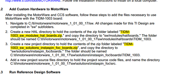
关于参考方案TIDM-1003的固件压缩包

$
0
0

TI的电动车控制器方案里的固件压缩包再哪?参考文案里提及的两个压缩包我都没找到?请教一下再哪下载?

硬件偏移校准(drv 8301 revd)

$
0
0

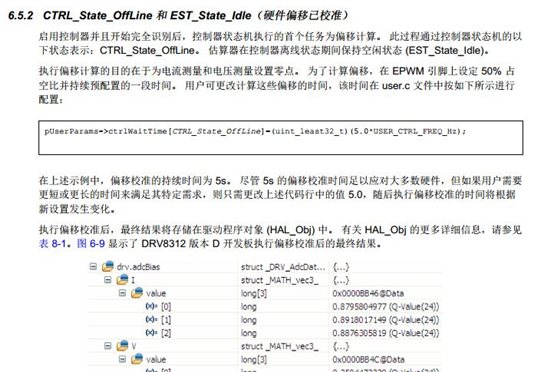
1、执行偏移计算的目的在于为电流测量和电压测量设置零点。这句话的含义:硬件偏移是不是在电机启动前,校准运放TLV2781偏离1.65V时的硬件校准?如果不是,这句话怎么理解?

2、在电机启动前,运放TLV2781严重偏离1.65V时,软件怎么补偿保证电机采样电流正确?

cmd文件一直报错

$
0
0

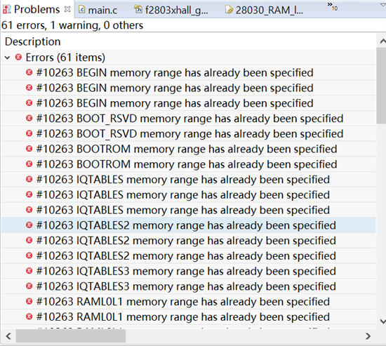
我在把工程导入之后,出现了很多问题,但是这个工程在别人的笔记本上是可以运行成功的,报错的地点是cmd文件出现了问题,说是重复定义了,请各位大神能帮忙解决一下,谢谢了!

加入工程后,总是显示重新定义了是怎么回事??

$
0
0

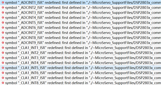
加入工程之后,一直报错,显示有符号重新定义了,如图所示。说第一次定义是在DSP2803x_common/source/DSP2803x_DefaultIsr.obj文件中,重新定义在 DSP2803x_common/source/DSP2803x_SWPrioritizedDefaultIsr.obj文件中。

F2808的ADC pin脚 内部是不是有上拉电阻?

$
0
0

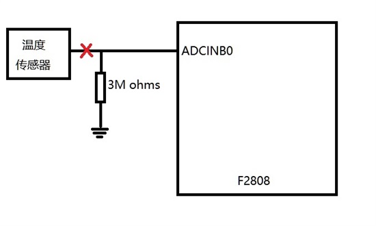
检测一个温度,当这个传感器断开连接后,相当于ADCINB0外接了个下拉3M电阻,理想情况,ADC转换值应该是接近为0。

但实际上这个电阻上竟然有0.5xxV的电压,导致ADC转换值错误。

咨询各高手,这DSP的ADC管脚内部电路是怎样的?

如何才能检测到接近0的值?

Viewing all 12114 articles
Browse latest View live


<script src="https://jsc.adskeeper.com/r/s/rssing.com.1596347.js" async> </script>